
Specialisation · Design · Manufacture · Lifecycle
Advanced PCB Design
The board is the product. Our senior electronics engineers deliver high-density, high-speed and RF layouts that pass compliance first time and yield on the line.
Discuss a PCB project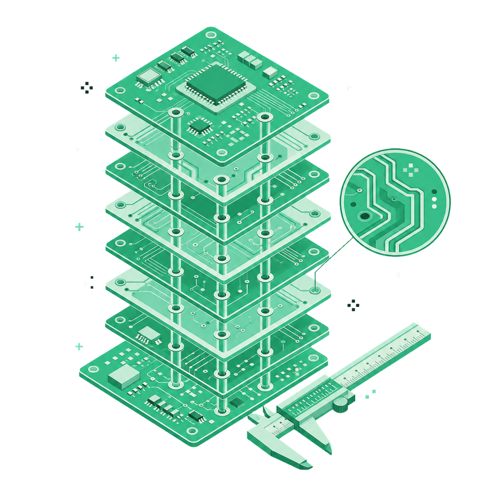
Why Tekt
Layouts engineered for physics, compliance and yield
Great schematics die in bad layout. Our PCB practice pairs simulation-driven signal and power integrity with the manufacturing knowledge of our own SMT line — every stack-up, via strategy and footprint decision is made knowing exactly how the board will be built and tested.
From high-density wearables to RF systems for Silentium Defence, our boards ship in medical, military and consumer products worldwide.
How we deliver
Unique value, end to end
Simulation first
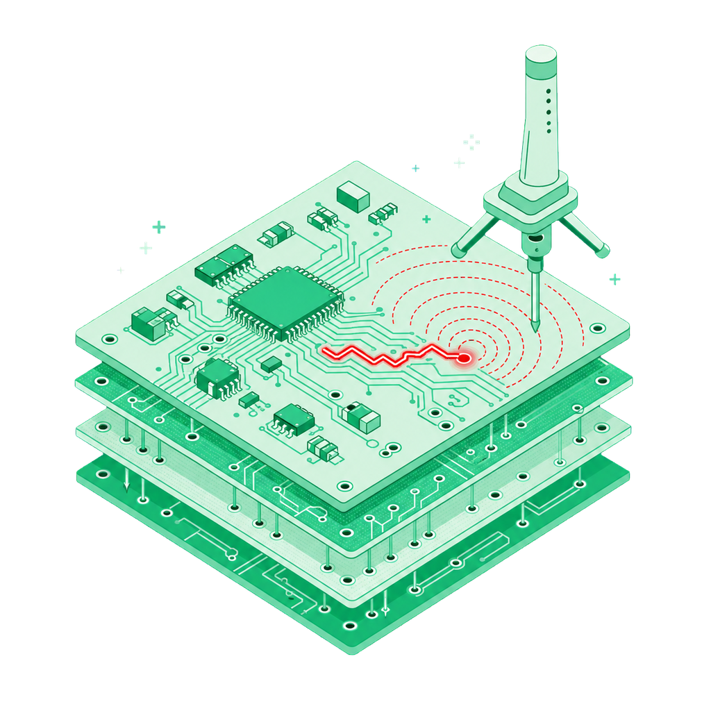
SI/PI and thermal simulation before fabrication — problems found on screen, not on the bench.
Built where designed
Layouts reviewed by the production engineers who will assemble them, on the line one floor down.
Compliance by design
EMC and safety margins engineered in from the first placement, pre-scanned in-house.
Case studies
Case studies
Real programs from this practice — the brief, the engineering approach, and where it landed.
- Case study 01 · Silentium Defence
RF front-end for passive radar
Passive radar lives or dies on noise floor. Our layouts for Silentium’s sensing platforms isolate sensitive RF chains from dense digital sections — qualified cleanly for defence deployment.
- Case study 02 · THIM
Wearable sleep-tracking hardware
A finger-worn wearable leaves no room for error. We delivered the miniaturised, power-frugal board design behind THIM’s sleep tracker, balancing radio performance against weeks-scale battery life.
- Case study 03 · Nano Components
High-speed IR sensing array
We re-engineered an existing IR solution into a new interference-based presence-sensing array — the analogue front end redesigned for high-speed detection at production-friendly cost.
What we solve
Problems this practice removes
- Boards that pass the bench but fail EMC
- Layouts that assemble poorly and yield worse
- High-speed interfaces marginal at temperature
- Re-spins driven by unobtainable parts
Tools, processes & standards

Who delivers it
The team behind it
- Senior PCB design engineer — 10+ years HDI and high-speed; medical and defence delivery
- Signal integrity specialist — Simulation correlated against lab measurement
- Production liaison engineer — Panelisation, test-point and yield ownership
Capabilities
FAQ
Frequently asked questions
Have a board that has to be right?
From first stack-up to first-pass compliance — we design boards that ship.
↑ Back to top